
Researchers at Osaka University have developed a groundbreaking flexible optical sensor that works even when crumpled. Using carbon nanotube photodetectors and wireless Bluetooth technology, this sensor enables non-invasive analysis and holds promise for advancements in imaging, wearable technology, and soft robotics. Credit: SciTechDaily.com
Researchers at Osaka University have created a soft, pliable, and wireless optical sensor using carbon nanotubes and organic transistors on an ultra-thin polymer film. This innovation is poised to open new possibilities in imaging technologies and non-destructive analysis techniques.
Recent years have brought remarkable progress in imaging technology, ranging from high-speed optical sensors capable of capturing more than two million frames per second to compact, lensless cameras that can capture images with just a single pixel.
In a study recently published in Advanced Materials, researchers from SANKEN (The Institute of Scientific and Industrial Research), at Osaka University have developed an optical sensor on an ultrathin, flexible sheet that can be bent without breaking. In fact, this sensor is so flexible, it will work even after it has been crumpled into a ball.
In a camera, the optical sensor is the device that senses the light that has passed through a lens, similar to the retina inside a human eye.
Innovations in Sensor Design
“Conventional optical sensors are built using inorganic <span class="glossaryLink" aria-describedby="tt" data-cmtooltip="
” data-gt-translate-attributes=”[{"attribute":"data-cmtooltip", "format":"html"}]” tabindex=”0″ role=”link”>semiconductors and ferroelectric materials,” says Rei Kawabata, lead author of the study. “This makes the sensors stiff and unable to bend. To avoid this problem, we looked at a different way to detect light.”
Instead of traditional light sensors, the researchers use an array of tiny carbon nanotube photodetectors printed on an ultra-thin polymer substrate (less than 5 μm). When exposed to light, the carbon nanotubes heat up, creating a thermal gradient that then generates a voltage signal. Doping the nanotubes with chemical carriers during printing further increases their sensitivity. Using these nanotubes, visible light as well as infrared light such as those related to heat or molecules can be measured.
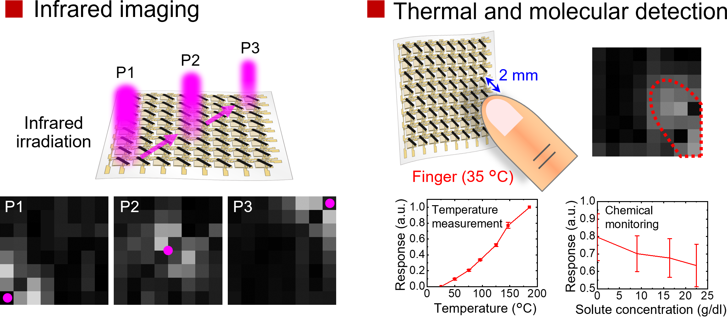
Detection and imaging of light, heat, and molecules using sheet-type optical sensors. Attribution 4.0 International (CC BY 4.0), Reprinted with permission from Advanced Materials. Credit: 2024 Araki et al., Ultraflexible Wireless Imager Integrated with Organic Circuits for Broadband Infrared Thermal Analysis, Advanced Materials
Wireless Technology Integration
Along with the carbon nanotube sensors, organic transistors are also printed on the polymer substrate to organize the voltage signals into an image signal. To read this signal, a computer does not need to be physically connected by wires to the sensor. Instead, a wireless Bluetooth module is used.
“Together with this wireless system, our imager can attach soft and curved objects to analyze their surfaces or insides without damaging them,” says Teppei Araki, senior author of the study.
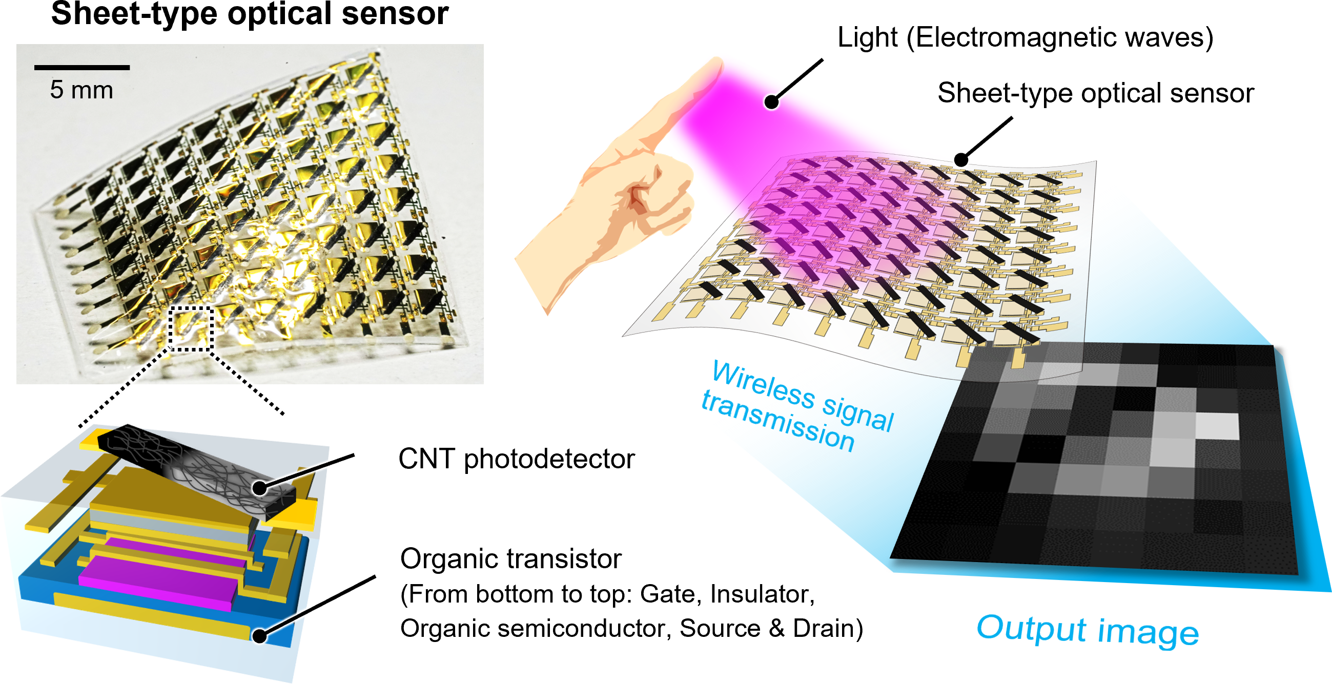
Sheet-type optical sensor integrated with a carbon nanotube photodetector and an organic transistor. Attribution 4.0 International (CC BY 4.0), Reprinted with permission from Advanced Materials. Credit: 2024 Araki et al., Ultraflexible Wireless Imager Integrated with Organic Circuits for Broadband Infrared Thermal Analysis, Advanced Materials
The researchers built a prototype of the sheet-type optical sensor and tested its ability to sense heat from objects like human fingers or wires as well as glucose flowing through tubes. They found the optical sensor has high sensitivity over a wide range of wavelengths. Moreover, at room temperature and atmospheric conditions, tests showed it has high bending durability and worked even after it was crumpled.
The unique advantages of this wireless measurement system and sheet-type optical sensor will lead to new and simpler ways to perform many tasks such as evaluating the quality of liquid without needing to sample it. The researchers believe it holds high promise in many applications such as non-destructive imaging, wearable devices, and soft robotics.
Reference: “Ultraflexible Wireless Imager Integrated with Organic Circuits for Broadband Infrared Thermal Analysis” by Rei Kawabata, Kou Li, Teppei Araki, Mihoko Akiyama, Kaho Sugimachi, Nozomi Matsuoka, Norika Takahashi, Daiki Sakai, Yuto Matsuzaki, Ryo Koshimizu, Minami Yamamoto, Leo Takai, Ryoga Odawara, Takaaki Abe, Shintaro Izumi, Naoko Kurihira, Takafumi Uemura, Yukio Kawano and Tsuyoshi Sekitani, 11 January 2024, Advanced Materials.
DOI: 10.1002/adma.202309864
The study was funded by the Japan Society for the Promotion of Science and the Japan Science and Technology Agency.