Scientists have developed perovskite crystals that could revolutionize optical technologies by facilitating efficient room-temperature operations in devices essential for advanced signal processing.
Integrated photonic circuits operating at room temperature combined with optical nonlinear effects could revolutionize both classical and quantum signal processing. Scientists from the Faculty of Physics at the University of Warsaw, in collaboration* with other institutions from Poland as well as Italy, Iceland, and Australia, have demonstrated the creation of perovskite crystals with predefined shapes that can serve in nonlinear photonics as waveguides, couplers, splitters, and modulators.
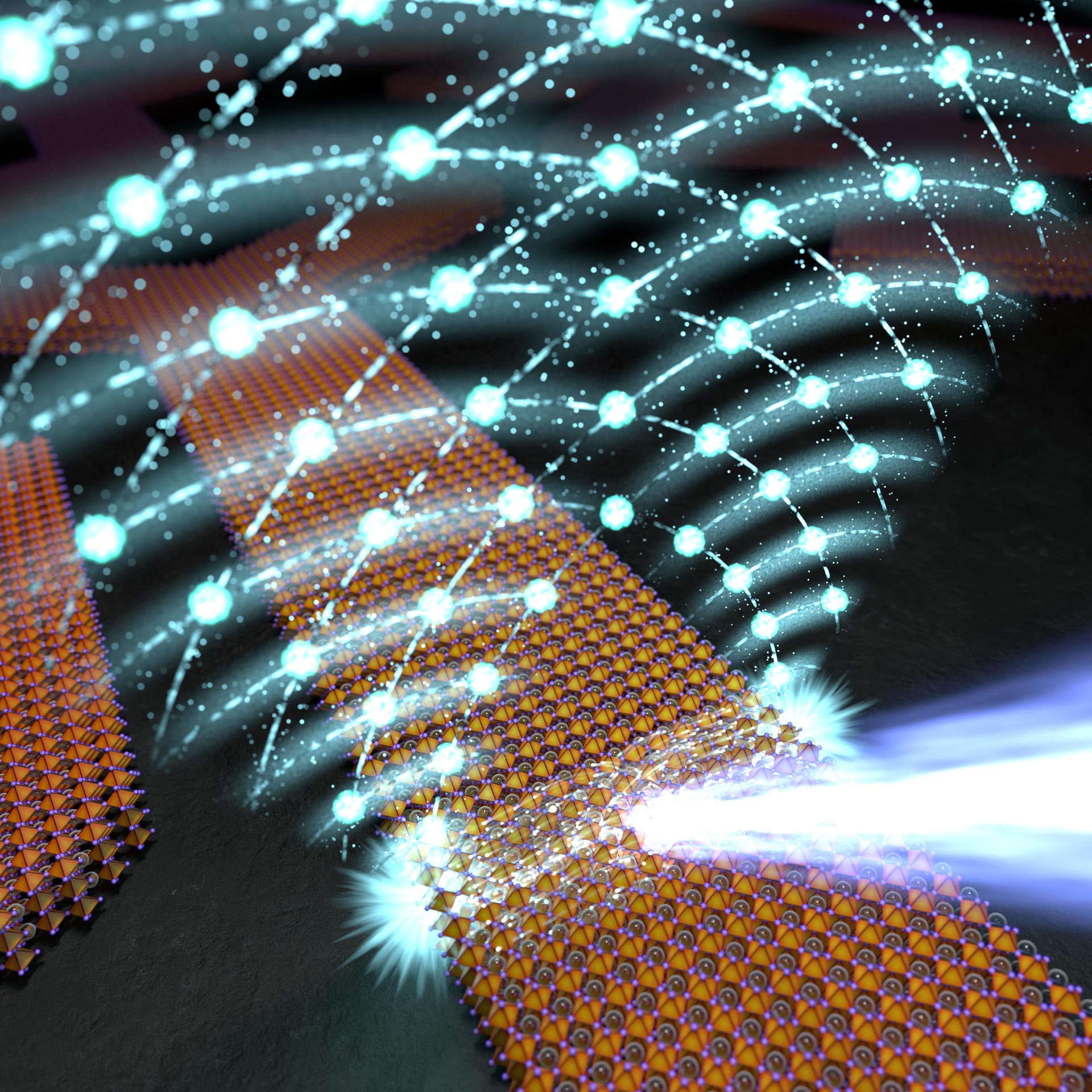
The research results, published in the prestigious journal Nature Materials, describe the fabrication of these innovative structures and the edge lasing effect. In particular, this effect is associated with the formation of the condensate of exciton-polaritons, which are quasiparticles behaving partly like light and partly like matter.
Harnessing Perovskites for Enhanced Optical Applications
Professor Barbara Piętka from the Faculty of Physics at the University of Warsaw, one of the project’s initiators and responsible for the research process, emphasizes that “perovskites exhibit great versatility: from polycrystalline layers, nano- and micro-crystals to bulk crystals. They can be used in various applications, from solar cells to lasers.
“Some, such as the CsPbBr3 (cesium-lead-bromide) material we used, are also ideal <span class="glossaryLink" aria-describedby="tt" data-cmtooltip="
” data-gt-translate-attributes=”[{"attribute":"data-cmtooltip", "format":"html"}]” tabindex=”0″ role=”link”>semiconductors for optical applications due to their high exciton binding energy and oscillator strength. These effects allow for enhanced light interactions, significantly lowering the energy required for nonlinear light amplification.”
Innovations in Crystal Synthesis Techniques
The researchers applied repeatable and scalable synthesis methods to obtain perovskite crystals with precisely defined dimensions and shapes. They used a microfluidic approach, where crystals are grown from a solution in narrow polymer molds that can be imprinted with any shape from a template. A key element was controlling the solution concentration and growth temperatures while maintaining an atmosphere of saturated solvent vapors.
This approach, combined with the use of nearly atomically smooth gallium arsenide templates made using electron-beam lithography and <span class="glossaryLink" aria-describedby="tt" data-cmtooltip="
” data-gt-translate-attributes=”[{"attribute":"data-cmtooltip", "format":"html"}]” tabindex=”0″ role=”link”>plasma etching at the Łukasiewicz Research Network – Institute of Microelectronics and Photonics under Anna Szerling’s leadership, produced high-quality single crystals. In this way, CsPbBr3 crystals can be formed into any shape with simple corners to smooth curves, which is a true achievement in the world of crystalline materials. They can be fabricated on any substrate, enhancing their compatibility with existing photonic devices.
Mateusz Kędziora, a doctoral student at the Faculty of Physics University of Warsaw and the first author of the paper who developed the crystal synthesis methods, adds, “These crystals, due to their high quality, form Fabry-Pérot type resonators on their walls, allowing strong nonlinear effects to be observed without the need for external Bragg mirrors,” which offers hope for the application of these materials in integrated photonic circuits.
Breakthroughs in Polaritonic Lasing and Condensate Formation
The demonstration of polaritonic lasing from the interfaces and corners of microwires marks another breakthrough.
“The wavelength of the emitted light is modified by the effects of strong light-matter interactions, indicating that the emission is due to the formation of a non-equilibrium Bose-Einstein condensate of exciton-polaritons. This is therefore not conventional lasing due to the Purcell effect (weak coupling), but emission from a condensate in the strong light-matter coupling regime,” explains Barbara Piętka.
“The high coherence between different signals of the emitted light from the edges and corners, confirmed in far-field photoluminescence and angle-resolved spectroscopy, indicates the formation of a coherent, macroscopically extended polariton condensate,” adds Dr. Helgi Sigurðsson from Faculty of Physics University of Warsaw and the Science Institute at the University of Iceland in Reykjavik.
Additional confirmation of nonlinear effects is the increase in energy with increasing population of a given mode (known as blueshift), which is a result of interactions within the condensate. Thanks to the unique properties of perovskite structures, the condensate can travel long distances within the crystals, and the emitted light can propagate through air gaps to neighboring structures.
Impact on Future Photonic Devices and Technology
“Our simulations show how naturally formed resonators for light modes and scattering affect the emission from edges and bends in the crystals,” adds Dr. Andrzej Opala from Faculty of Physics University of Warsaw and Institute of Physics of the Polish Academy of Sciences, one of the main authors of the paper and the developer of the theoretical model showing how numerical aperture and spatial confinement in microwires affect the observed effects.
“Furthermore, thanks to calculations based on solving Maxwell’s equations in three-dimensional structures with complex shapes, we were able to visualize photonic modes and show how their image forms in the far field,” explains Prof. Tomasz Czyszanowski from Lodz University of Technology, who specializes in simulations of photonic and laser structures.
The discovery allows for their use in compact “on-chip” systems that can handle both classical and <span class="glossaryLink" aria-describedby="tt" data-cmtooltip="
” data-gt-translate-attributes=”[{"attribute":"data-cmtooltip", "format":"html"}]” tabindex=”0″ role=”link”>quantum computing tasks.
“We predict that our discoveries will open the door to future devices that can operate at the level of single photons, integrating nanolasers with waveguides and other elements on a single chip,” concludes Prof. Michał Matuszewski from the Center for Theoretical Physics of the Polish Academy of Sciences.
Integration and Commercialization Prospects of Perovskite Photonic Technologies
Perovskites could play a key role in the further development of optical technologies, and the discoveries of physicists from UW could significantly increase the chances of using perovskite crystals in nonlinear photonics operating at room temperature. Moreover, the developed structures may be compatible with silicon technology, further enhancing their commercialization potential.
Reference: “Predesigned perovskite crystal waveguides for room-temperature exciton–polariton condensation and edge lasing” by Mateusz Kędziora, Andrzej Opala, Rosanna Mastria, Luisa De Marco, Mateusz Król, Karolina Łempicka-Mirek, Krzysztof Tyszka, Marek Ekielski, Marek Guziewicz, Karolina Bogdanowicz, Anna Szerling, Helgi Sigurðsson, Tomasz Czyszanowski, Jacek Szczytko, Michał Matuszewski, Daniele Sanvitto and Barbara Piętka, 19 August 2024, Nature Materials.
DOI: 10.1038/s41563-024-01980-3
*Research conducted at the Faculty of Physics, University of Warsaw (UW) in collaboration with the Institute of Physics of the Polish Academy of Sciences (IFPAN), the Institute of Nanotechnology CNR-Nanotec in Lecce, Italy, the School of Physics at the <span class="glossaryLink" aria-describedby="tt" data-cmtooltip="
” data-gt-translate-attributes=”[{"attribute":"data-cmtooltip", "format":"html"}]” tabindex=”0″ role=”link”>Australian National University in Canberra (UAu), the Łukasiewicz Research Network – Institute of Microelectronics and Photonics (Łukasiewicz-IMiF), the Institute of Physics at the Lodz University of Technology (PŁ), the Science Institute at the University of Iceland in Reykjavik (UIs), and the Center for Theoretical Physics of the Polish Academy of Sciences (CFT PAN).