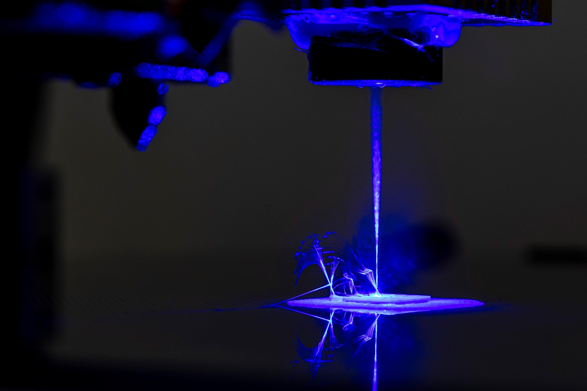
University of Missouri researchers have developed a novel 3D printing method that allows the creation of complex multi-material devices in a single process, streamlining manufacturing and enhancing environmental sustainability. Credit: Sam O’Keefe
An innovative 3D printing method simplifies the manufacturing of multi-material products.
Researchers at the University of Missouri have developed a method to create complex devices with multiple materials — including plastics, metals, and <span class="glossaryLink" aria-describedby="tt" data-cmtooltip="
” data-gt-translate-attributes=”[{"attribute":"data-cmtooltip", "format":"html"}]” tabindex=”0″ role=”link”>semiconductors – all with a single machine.
The research, which was recently published in <span class="glossaryLink" aria-describedby="tt" data-cmtooltip="
” data-gt-translate-attributes=”[{"attribute":"data-cmtooltip", "format":"html"}]” tabindex=”0″ role=”link”>Nature Communications, outlines a novel 3D printing and laser process to manufacture multi-material, multi-layered sensors, circuit boards, and even textiles with electronic components.
It’s called the Freeform Multi-material Assembly Process, and it promises to revolutionize the fabrication of new products.
By printing sensors embedded within a structure, the machine can make things that can sense environmental conditions, including temperature and pressure. For other researchers, that could mean having a natural-looking object such as a rock or seashell that could measure the movement of ocean water. For the public, applications could include wearable devices that monitor blood pressure and other vital signs.
Advancements in 3D Printing Techniques
Specifically, other techniques fall short when it comes to how versatile the material can be and how precisely smaller components can be placed inside larger 3D structures.
The Mizzou team’s method uses special techniques to solve these problems. Team members built a machine that has three different nozzles: one adds ink-like material, another uses a laser to carve shapes and materials, and the third adds additional functional materials to enhance the product’s capabilities. It starts by making a basic structure with regular 3D printing filament, such as polycarbonate, a type of transparent thermoplastic. Then, it switches to laser to convert some parts into a special material called laser-induced <span class="glossaryLink" aria-describedby="tt" data-cmtooltip="
” data-gt-translate-attributes=”[{"attribute":"data-cmtooltip", "format":"html"}]” tabindex=”0″ role=”link”>graphene, putting it exactly where it’s needed. Finally, more materials are added to enhance the functional abilities of the final product.
This work is being funded by the National Science Foundation (NSF) Advanced Manufacturing program, and the NSF I-CorpsTM program is providing funds to explore commercialization.
“The I-Corps program is helping us identify market interests and needs,” Lin said. “Currently, we believe it would be of interest to other researchers, but we believe it will ultimately benefit businesses. It will shorten fabrication time for device prototyping by allowing companies to make prototypes in-house. This technology, available only at Mizzou, shows great promise for transforming the way products are fabricated and manufactured.”
“This is the first time this type of process has been used, and it’s unlocking new possibilities,” said Bujingda Zheng, a doctoral student in mechanical engineering at Mizzou and the lead author of the study. “I’m excited about the design. I’ve always wanted to do something that no one has ever done before, and I’m getting to do that here at Mizzou.”
One of the main benefits is that innovators can focus on designing new products without worrying about how to prototype them.
“This opens the possibility for entirely new markets,” said Jian “Javen” Lin, an associate professor of mechanical and aerospace engineering at Mizzou. “It will have broad impacts on wearable sensors, customizable robots, medical devices, and more.”
Revolutionary techniques
Currently, manufacturing a multi-layered structure — such as a printed circuit board — can be a cumbersome process that involves multiple steps and materials. These processes are costly, time-consuming, and can generate waste that harms the environment.
Not only is the new technique better for the planet, it’s inspired by systems found in nature.
“Everything in nature consists of structural and functional materials,” Zheng said. “For example, electrical eels have bones and muscles that enable them to move. They also have specialized cells that can discharge up to 500 volts to deter predators. These biological observations have inspired researchers to develop new methods for fabricating 3D structures with multi-functional applications, but other emerging methods have limitations.”
Reference: “Programmed multimaterial assembly by synergized 3D printing and freeform laser induction” by Bujingda Zheng, Yunchao Xie, Shichen Xu, Andrew C. Meng, Shaoyun Wang, Yuchao Wu, Shuhong Yang, Caixia Wan, Guoliang Huang, James M. Tour and Jian Lin, 28 May 2024, Nature Communications.
DOI: 10.1038/s41467-024-48919-5